

A brand new epitaxial mechanism permits ultra-high high quality Ag movies on Cu substrates

It’s simple to provide polycrystalline metallic movies on wafers however producing single‑crystal metallic movies is much more difficult. As a result of single crystals don’t have any grain boundaries (the joints between otherwise oriented crystal areas in polycrystalline supplies), they provide a lot better electrical efficiency: larger conductivity, decrease resistive losses, improved excessive‑frequency behaviour (vital for prime‑velocity communication and 5G), and decreased noise for quantum applied sciences. In consequence, strategies for reliably producing single‑crystal movies are extremely wanted.
Single‑crystal silver and copper movies are significantly priceless. Silver is an distinctive conductor of each electrical energy and light-weight, whereas copper gives glorious thermal administration and reduces resistive heating. Nonetheless, rising silver on copper is notoriously tough as a result of the 2 supplies have a big lattice mismatch (13%), which usually introduces pressure, defects, dislocations, and tough, low‑high quality movies. This makes typical epitaxy primarily unattainable.
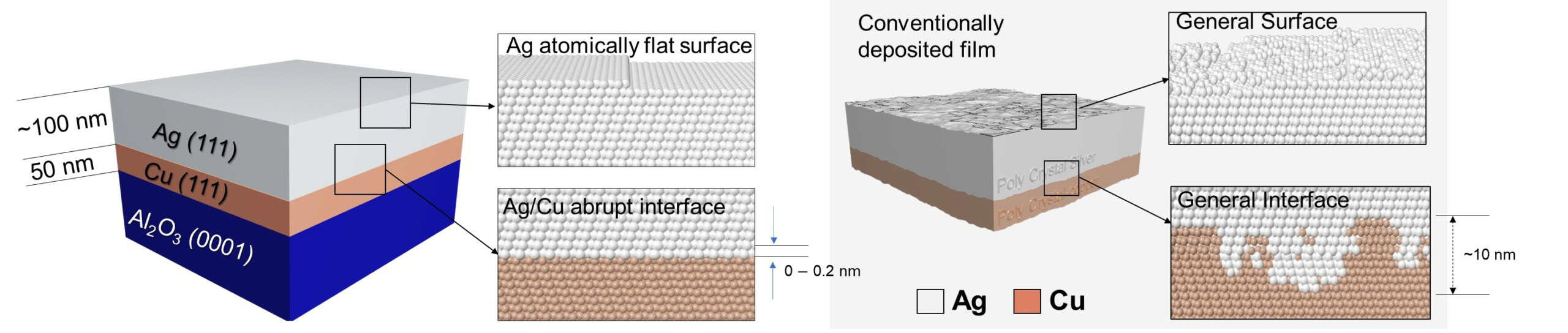
On this work, the researchers overcame this barrier utilizing Atomic Sputtering Epitaxy, which permits exact atomic deposition, mixed with publish‑annealing to cut back twin boundaries. They found that the mismatch pressure is absorbed totally inside the first atomic layer of silver. This happens as a result of the atoms on the interface shift sideways in a periodic, managed sample that releases the pressure. This represents a brand new type of heteroepitaxy wherein two supplies with completely different lattice periodicities can nonetheless develop collectively seamlessly.
They demonstrated wafer‑scale, defect‑free single‑crystal silver movies on copper regardless of the large lattice mismatch, enabling extremely‑excessive high quality metallic movies for superior optical and digital applied sciences. This method opens the door to new heteroepitaxial programs and gives a path to producing silver movies with distinctive optical and digital efficiency.
“What we discover most notable is {that a} 13% lattice mismatch, which might usually forestall clear heteroepitaxy, is absorbed nearly totally inside the first monoatomic Ag layer on the Ag/Cu interface, permitting the movie above to develop as if by itself native lattice and yielding wafer-scale, grain-boundary-free movies with atomically flat surfaces. We hope this idea of a strain-absorbing monolayer interface will be prolonged to different dissimilar metallic pairs.” – Professor Younger-Min Kim, Sungkyunkwan College
Do you need to study extra about this subject?
Si/Ge nanostructures by Karl Brunner (2001)