

A brand new machine studying workflow helps decode low-loss EELS knowledge, turning noisy nanoscale spectra into spatial maps of the optical resonances that form next-generation hybrid nanophotonic supplies.

Paper: Extremely environment friendly machine studying technique for low-loss eels characterization: nanophotonic resonances as a case examine. Picture Credit score: AI-generated picture / OpenAI
In a current analysis article revealed within the journal npj Computational Supplies, researchers developed a extremely environment friendly machine studying technique that mixes unsupervised and supervised algorithms to categorise and interpret low-loss electron power loss spectroscopy (EELS) knowledge and to spatially map complicated nanophotonic resonances in silicon/gold nanopillars.
Nanoscale Spectroscopy Challenges
The characterization of nanoscale supplies typically depends on probing their bodily, chemical, and digital properties with excessive spatial decision. Electron energy-loss spectroscopy (EELS) mixed with scanning transmission electron microscopy (STEM) is a useful method on this regard, offering spatially resolved spectra that mirror materials properties.
Significantly, the low-loss area of EELS spectra (under 50 eV) incorporates info on collective excitations, corresponding to plasmons and Mie resonances, in addition to inter- and intra-band digital transitions and phonon excitations. These low-energy excitations are essential for understanding nanophotonic results in hybrid metal-semiconductor nanostructures.
Nonetheless, analyzing low-loss EELS knowledge is difficult as a result of a number of elements inherent to the nanoscale regime: overlapping spectral resonances, the extraordinary zero-loss peak (ZLP) that masks close by options, and low signal-to-noise ratio in small volumes.
Conventional evaluation strategies corresponding to Principal Part Evaluation (PCA) and Non-negative Matrix Factorization (NMF) help with denoising and dimensionality discount however typically lack adaptive studying and predictive capabilities.
With current advances producing massive, complicated datasets, implementing sturdy, automated machine studying (ML) methods tailor-made to low-loss EELS is critical to allow extra correct and environment friendly characterization of nanophotonic resonances and different excitations.
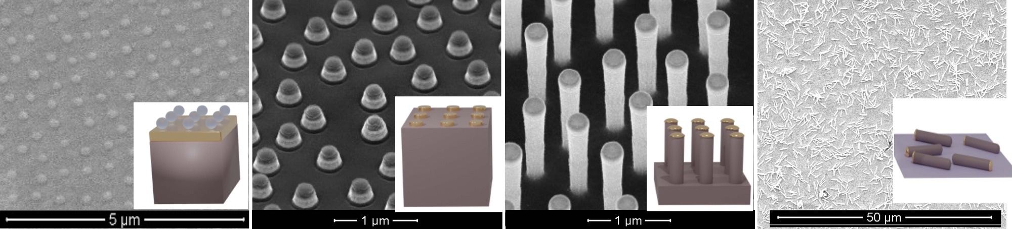
Schematic illustration and SEM photos of the fabrication strategy of the Si/Au nanopillars by colloidal lithography. (a) Array of polystyrene nanospheres homogeneously self assembled on the Au floor on prime of the silicon wafer. (b) Au nanodiscs obtained by Ar RIE utilizing the nanospheres as masks. (c) Obtained Si/Au nanopillars by deep Si RIE utilizing the Au nanodiscs as masks. (d) Nanopillars after their launch from the substrate by ultrasounds.
Machine Studying Workflow
Step one employs Uniform Manifold Approximation and Projection (UMAP), a nonlinear dimensionality discount algorithm, to remodel the high-dimensional spectral knowledge right into a lower-dimensional house, preserving the complicated nonlinear relationships attribute of low-loss EELS indicators.
Subsequently, Hierarchical Density-Primarily based Spatial Clustering of Functions with Noise (HDBSCAN), an unsupervised clustering technique, is utilized to the lowered representations to determine clusters akin to completely different native spectral profiles.
Because of the presence of outliers or uncommon spectral patterns, a ultimate supervised classification step utilizing Help Vector Machines (SVM) is launched to reclassify these ambiguous factors, leveraging the clusters obtained by HDBSCAN as labeled coaching knowledge. This hybrid unsupervised-supervised workflow allows near-real-time classification of huge datasets and helps transferability to new EELS maps acquired below comparable experimental situations with out retraining from scratch.
Experimentally, Si/Au nanopillars have been fabricated utilizing colloidal lithography and reactive ion etching, producing p-doped Si nanopillars roughly 200 nm in diameter and a couple of μm lengthy, capped with 75 nm thick Au nanodiscs. STEM-EELS measurements have been carried out at 60 keV with excessive spatial decision, yielding spectrum photos that seize spatially localized nanophotonic resonances.
Complementary finite-difference time-domain (FDTD) simulations modeled the optical absorption of the nanopillars below aircraft wave illumination to correlate EELS resonances with electromagnetic modes, whereas recognizing that EELS can probe further modes past these excited by aircraft waves.
Resonance Mapping Insights
Making use of the mixed UMAP-HDBSCAN-SVM evaluation to high-resolution low-loss EELS knowledge revealed distinct clusters that may very well be related to spatially localized nanophotonic resonances throughout the Si/Au nanopillars. The strategy successfully separated vacuum/background and nanopillar areas from areas exhibiting attribute plasmonic, hybrid, and dielectric resonances after ZLP exclusion.
Notably, the EELS spectra close to 2.45 eV localized on the Au nanodisc have been interpreted not as a single optical mode however fairly as a cluster of intently spaced resonances, in step with FDTD simulations and presumably influenced by identified interband transitions in Au. This illustrates the ML technique’s means to resolve complicated nanoscale resonance clusters which might be tough to differentiate with standard approaches.
A reproducibility check on an impartial spectrum picture from the sting of one other nanopillar confirmed the robustness of the technique, efficiently figuring out related attribute clusters and associated nanophotonic modes.
Extra evaluation of lower-magnification photos, the place spatial decision and sign energy have been lowered, demonstrated that, regardless of these limitations, the strategy nonetheless detected and localized nanophotonic resonances, highlighting its sensitivity and adaptableness to various experimental situations. Nonetheless, the lower-resolution knowledge couldn’t resolve the finer resonance particulars noticed in high-resolution measurements.
The supervised SVM stage proved instrumental in extending the unsupervised clustering by assigning outlier spectra throughout the dataset to acceptable lessons, thus enhancing the completeness and accuracy of the classification. Its means to generalize from one dataset to impartial acquisitions below related experimental situations additional suggests applicability for speedy on-the-fly EELS knowledge interpretation.
The mixture of excessive spatial-resolution STEM-EELS with this environment friendly ML framework opens new avenues for unraveling complicated nanophotonic phenomena, together with plasmon-Mie hybridization and dielectric mode coupling in hybrid nanostructures.
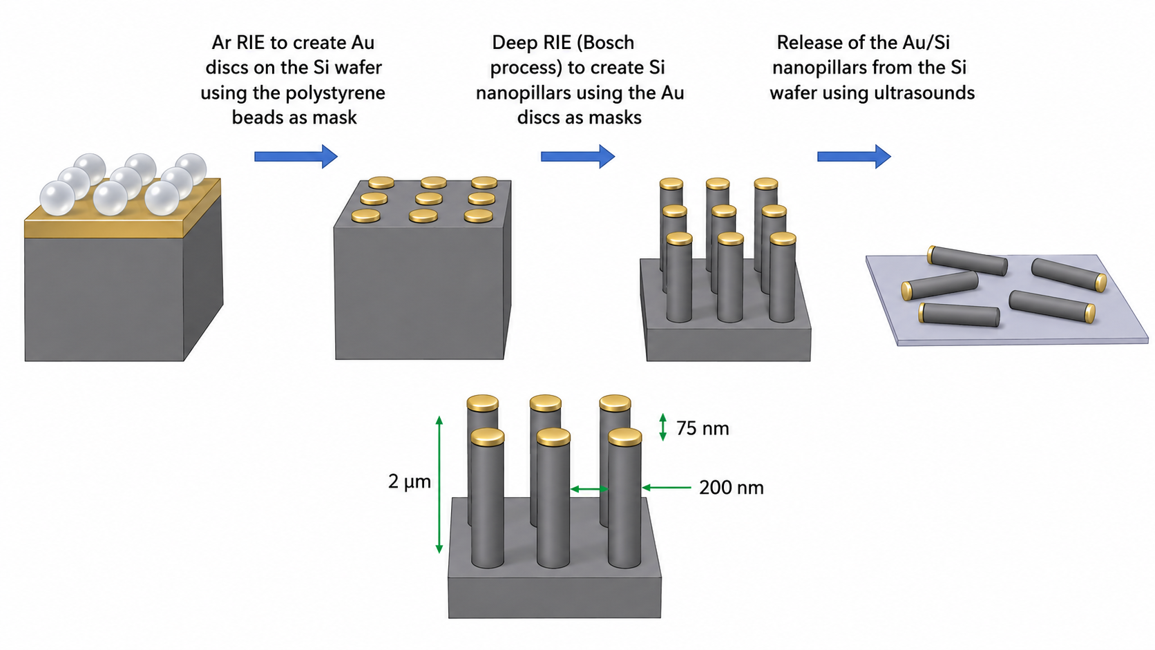
Schematic of Si/Au nanopillar fabrication. Ar RIE to create Au nanodiscs on the Si wafer utilizing polystyrene beads as masks. Deep RIE (Bosch course of) to type Si nanopillars utilizing the Au discs as masks. Launch of the Au/Si nanopillars from the Si wafer by ultrasonication and schematic of the size. Picture Credit score: Tailored from Costa-Ledesma, V., del-Pozo-Bueno, D., Coll, C. et al. (2026). Extremely environment friendly machine studying technique for low-loss EELS characterization: nanophotonic resonances as a case examine. npj Computational Supplies. DOI: 10.1038/s41524-026-02171-1. Licensed below CC BY 4.0.
Advances and Functions
This examine demonstrates a extremely environment friendly machine studying technique combining UMAP for dimensionality discount, HDBSCAN for unsupervised clustering, and SVM for supervised refinement to research low-loss EELS spectrum photos of nanoscale hybrid metal-semiconductor constructions.
The methodology displays robustness throughout completely different datasets and experimental situations, together with lower-magnification measurements, and supplies a transferable mannequin for speedy classification of latest EELS acquisitions when experimental situations are comparable.
By enabling automated, near-real-time classification and supporting the interpretation of complicated excitation modes on the nanoscale, this work paves the best way for superior characterization of nanostructured supplies.
Obtain your PDF copy by clicking right here.
Supply:
- Costa-Ledesma V., del-Pozo-Bueno D., et al. (2026). Extremely environment friendly machine studying technique for low-loss EELS characterization: nanophotonic resonances as a case examine. npj Computational Supplies. DOI: 10.1038/s41524-026-02171-1, https://www.nature.com/articles/s41524-026-02171-1