

Skoltech researchers and their colleagues from Ludwig Maximilian College of Munich, Germany, Nanjing College of China, and the Nationwide Institute for Supplies Science of Japan have developed a way for depositing natural molecules on a two-dimensional semiconductor in a extremely managed method. Examined on this proof-of-concept research, the approach makes use of self-assembled DNA origami nanostructures to hold natural dye molecules in a predefined sample lined by a 2D semiconductor. Sooner or later, the approach may very well be used to create parts for ultrasmall high-performance units. The analysis paper got here out within the journal Small Strategies.

Initially impressed by graphene, a brand new class of atomically skinny semiconductor supplies – akin to molybdenum disulfide – guarantees to allow digital and optical units which are smaller and extra environment friendly than these achievable with typical semiconductors like silicon. Nevertheless, working at such a small scale introduces a big nanopatterning problem: Creating well-defined, useful pathways inside a two-dimensional materials requires a stage of precision that pushes the bounds of present fabrication strategies.
“There are two fundamental approaches to making a ‘panorama’ on a 2D semiconductor sheet to information the conduction of excitons alongside most popular paths: Both you introduce some form of defects that alter the initially uniform construction of the fabric, which is thus far not potential to do with nanometer precision, or you deposit natural molecules on the monolayer, however till now it hasn’t been finished in a managed method, and the randomness of the ensuing sample places a limitation on the system effectivity,” stated research co-author Assistant Professor Irina Martynenko from Skoltech Physics.
The group efficiently demonstrated a method of depositing natural dye molecules on a monolayer of molybdenum disulfide utilizing the strategy of DNA origami. It entails designing DNA nanostructures roughly 100 nanometers in measurement that carry dye molecules at predefined positions. The ensuing assemble is positioned on a chip and lined by a 2D semiconductor.
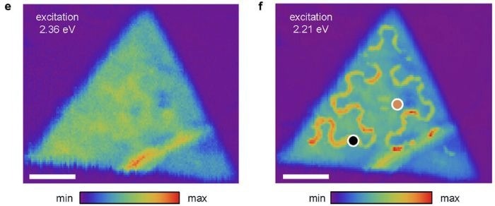
Picture. Photoluminescence map of a triangular flake of atomically skinny molybdenum disulfide with (proper) and with out (left) the underlying DNA origami-dye sample’s contribution. The dye molecules carried by DNA clearly have an effect on gentle emission throughout the flake. Credit score: Shen Zhao et al./Small Strategies
“Our experiments present that, firstly, the DNA origami-dye constructions do assemble appropriately and, second, the dye molecules and the molybdenum disulfide monolayer certainly exhibit the phenomenon of Förster resonance power switch. That is what permits the power alternate between the 2 supplies and due to this fact permits the semiconductor’s properties to be structured on the nanoscale by the deposited sample. You possibly can see this in photoluminescence pictures the place a triangular molybdenum disulfide flake shows kind of uniform gentle emission at a wavelength not related for the dye molecules deposited behind the flake, however clearly emits extra gentle in areas the place the dye molecules soak up gentle,” stated one of many research’s authors, Affiliate Professor Anvar Baimuratov from Skoltech Physics.
Now that the group has confirmed that DNA origami can be utilized to exactly and reliably sample the power panorama of two-dimensional semiconductors on the nanoscale, the researchers will try to create particular nanoelectronic and nanophotonic units utilizing this system. Finally, such nanostructured hybrid supplies may allow the design of compact high-performance units for optical computation and quantum simulations, gentle detection, and so on.