

The electronics trade is approaching a restrict to the variety of transistors that may be packed onto the floor of a pc chip. So, chip producers wish to construct up slightly than out.
As a substitute of compacting ever-smaller transistors onto a single floor, the trade is aiming to stack a number of surfaces of transistors and semiconducting components — akin to turning a ranch home right into a high-rise. Such multilayered chips may deal with exponentially extra information and perform many extra complicated capabilities than at the moment’s electronics.
A major hurdle, nevertheless, is the platform on which chips are constructed. As we speak, cumbersome silicon wafers function the primary scaffold on which high-quality, single-crystalline semiconducting components are grown. Any stackable chip must embrace thick silicon “flooring” as a part of every layer, slowing down any communication between purposeful semiconducting layers.
Now, MIT engineers have discovered a means round this hurdle, with a multilayered chip design that doesn’t require any silicon wafer substrates and works at temperatures low sufficient to protect the underlying layer’s circuitry.
In a research showing at the moment within the journal Nature, the group reviews utilizing the brand new technique to manufacture a multilayered chip with alternating layers of high-quality semiconducting materials grown straight on prime of one another.
The tactic allows engineers to construct high-performance transistors and reminiscence and logic components on any random crystalline floor — not simply on the cumbersome crystal scaffold of silicon wafers. With out these thick silicon substrates, a number of semiconducting layers could be in additional direct contact, main to raised and sooner communication and computation between layers, the researchers say.
The researchers envision that the strategy may very well be used to construct AI {hardware}, within the type of stacked chips for laptops or wearable units, that will be as quick and highly effective as at the moment’s supercomputers and will retailer large quantities of information on par with bodily information facilities.
“This breakthrough opens up huge potential for the semiconductor trade, permitting chips to be stacked with out conventional limitations,” says research writer Jeehwan Kim, affiliate professor of mechanical engineering at MIT. “This might result in orders-of-magnitude enhancements in computing energy for purposes in AI, logic, and reminiscence.”
The research’s MIT co-authors embrace first writer Ki Seok Kim, Seunghwan Search engine optimization, Doyoon Lee, Jung-El Ryu, Jekyung Kim, Jun Min Suh, June-chul Shin, Min-Kyu Music, Jin Feng, and Sangho Lee, together with collaborators from Samsung Superior Institute of Expertise, Sungkyunkwan College in South Korea, and the College of Texas at Dallas.
Seed pockets
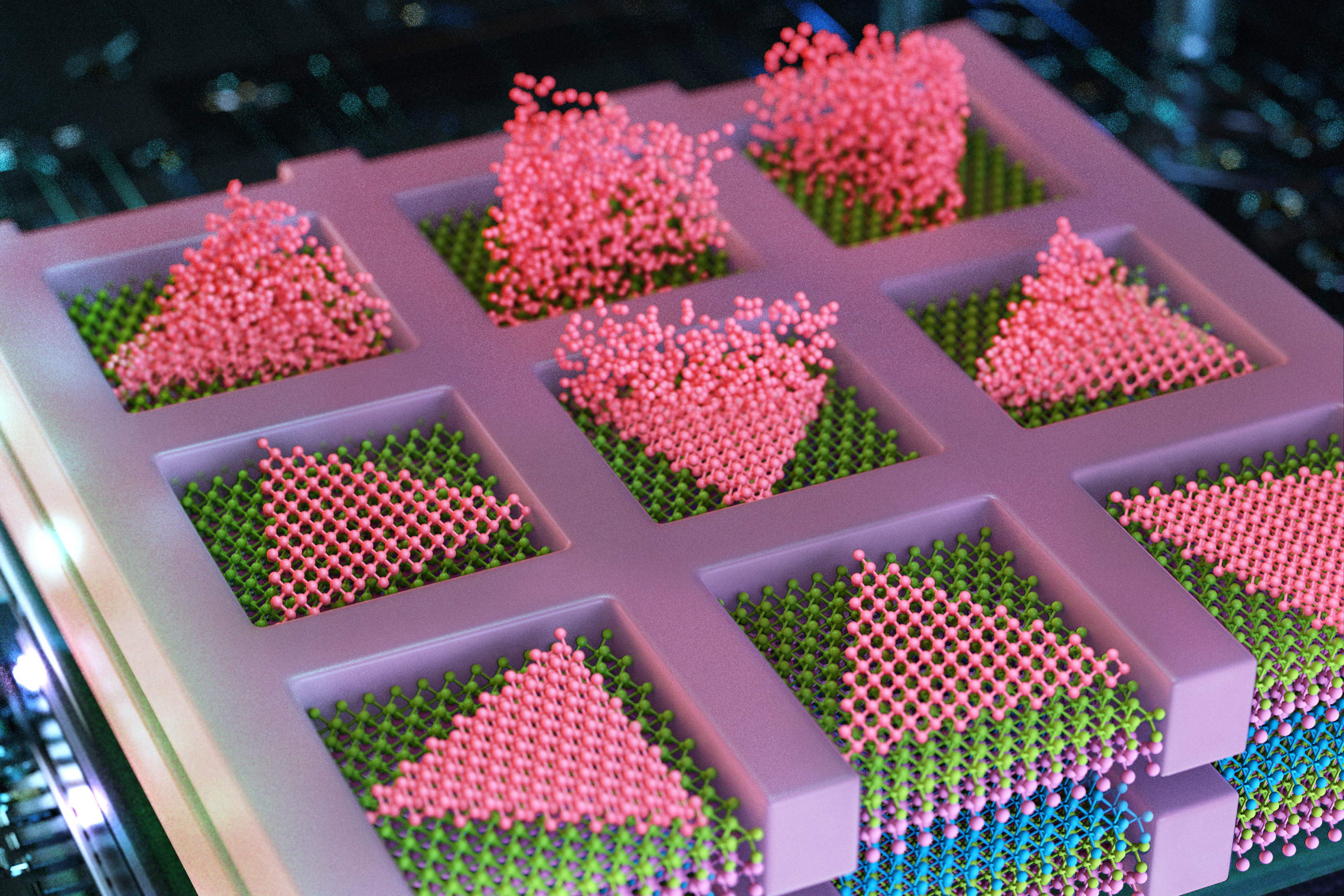
In 2023, Kim’s group reported that they developed a technique to develop high-quality semiconducting supplies on amorphous surfaces, much like the various topography of semiconducting circuitry on completed chips. The fabric that they grew was a kind of 2D materials often known as transition-metal dichalcogenides, or TMDs, thought of a promising successor to silicon for fabricating smaller, high-performance transistors. Such 2D supplies can keep their semiconducting properties even at scales as small as a single atom, whereas silicon’s efficiency sharply degrades.
Of their earlier work, the group grew TMDs on silicon wafers with amorphous coatings, in addition to over current TMDs. To encourage atoms to rearrange themselves into high-quality single-crystalline type, slightly than in random, polycrystalline dysfunction, Kim and his colleagues first coated a silicon wafer in a really skinny movie, or “masks” of silicon dioxide, which they patterned with tiny openings, or pockets. They then flowed a gasoline of atoms over the masks and located that atoms settled into the pockets as “seeds.” The pockets confined the seeds to develop in common, single-crystalline patterns.
However on the time, the strategy solely labored at round 900 levels Celsius.
“It’s important to develop this single-crystalline materials beneath 400 Celsius, in any other case the underlying circuitry is totally cooked and ruined,” Kim says. “So, our homework was, we needed to do the same method at temperatures decrease than 400 Celsius. If we may try this, the affect could be substantial.”
Build up
Of their new work, Kim and his colleagues seemed to fine-tune their technique with a view to develop single-crystalline 2D supplies at temperatures low sufficient to protect any underlying circuitry. They discovered a surprisingly easy answer in metallurgy — the science and craft of metallic manufacturing. When metallurgists pour molten metallic right into a mildew, the liquid slowly “nucleates,” or types grains that develop and merge right into a repeatedly patterned crystal that hardens into strong type. Metallurgists have discovered that this nucleation happens most readily on the edges of a mildew into which liquid metallic is poured.
“It’s recognized that nucleating on the edges requires much less power — and warmth,” Kim says. “So we borrowed this idea from metallurgy to make the most of for future AI {hardware}.”
The group seemed to develop single-crystalline TMDs on a silicon wafer that already has been fabricated with transistor circuitry. They first coated the circuitry with a masks of silicon dioxide, simply as of their earlier work. They then deposited “seeds” of TMD on the edges of every of the masks’s pockets and located that these edge seeds grew into single-crystalline materials at temperatures as little as 380 levels Celsius, in comparison with seeds that began rising within the middle, away from the sides of every pocket, which required larger temperatures to type single-crystalline materials.
Going a step additional, the researchers used the brand new technique to manufacture a multilayered chip with alternating layers of two totally different TMDs — molybdenum disulfide, a promising materials candidate for fabricating n-type transistors; and tungsten diselenide, a cloth that has potential for being made into p-type transistors. Each p- and n-type transistors are the digital constructing blocks for finishing up any logic operation. The group was in a position to develop each supplies in single-crystalline type, straight on prime of one another, with out requiring any intermediate silicon wafers. Kim says the strategy will successfully double the density of a chip’s semiconducting components, and notably, metal-oxide semiconductor (CMOS), which is a primary constructing block of a contemporary logic circuitry.
“A product realized by our method will not be solely a 3D logic chip but additionally 3D reminiscence and their mixtures,” Kim says. “With our growth-based monolithic 3D technique, you possibly can develop tens to lots of of logic and reminiscence layers, proper on prime of one another, and they might be capable to talk very effectively.”
“Standard 3D chips have been fabricated with silicon wafers in-between, by drilling holes by way of the wafer — a course of which limits the variety of stacked layers, vertical alignment decision, and yields,” first writer Kiseok Kim provides. “Our growth-based technique addresses all of these points without delay.”
To commercialize their stackable chip design additional, Kim has lately spun off an organization, FS2 (Future Semiconductor 2D supplies).
“We to date present an idea at a small-scale gadget arrays,” he says. “The subsequent step is scaling as much as present skilled AI chip operation.”
This analysis is supported, partially, by Samsung Superior Institute of Expertise and the U.S. Air Power Workplace of Scientific Analysis.