

Engineers on the College of Texas at Austin have constructed a table-top Excessive Ultraviolet lithography system and paired it with a brand new 3D printing method that reduces semiconductor nanostructure processing time from days to minutes, in line with a research printed in Nano Letters.
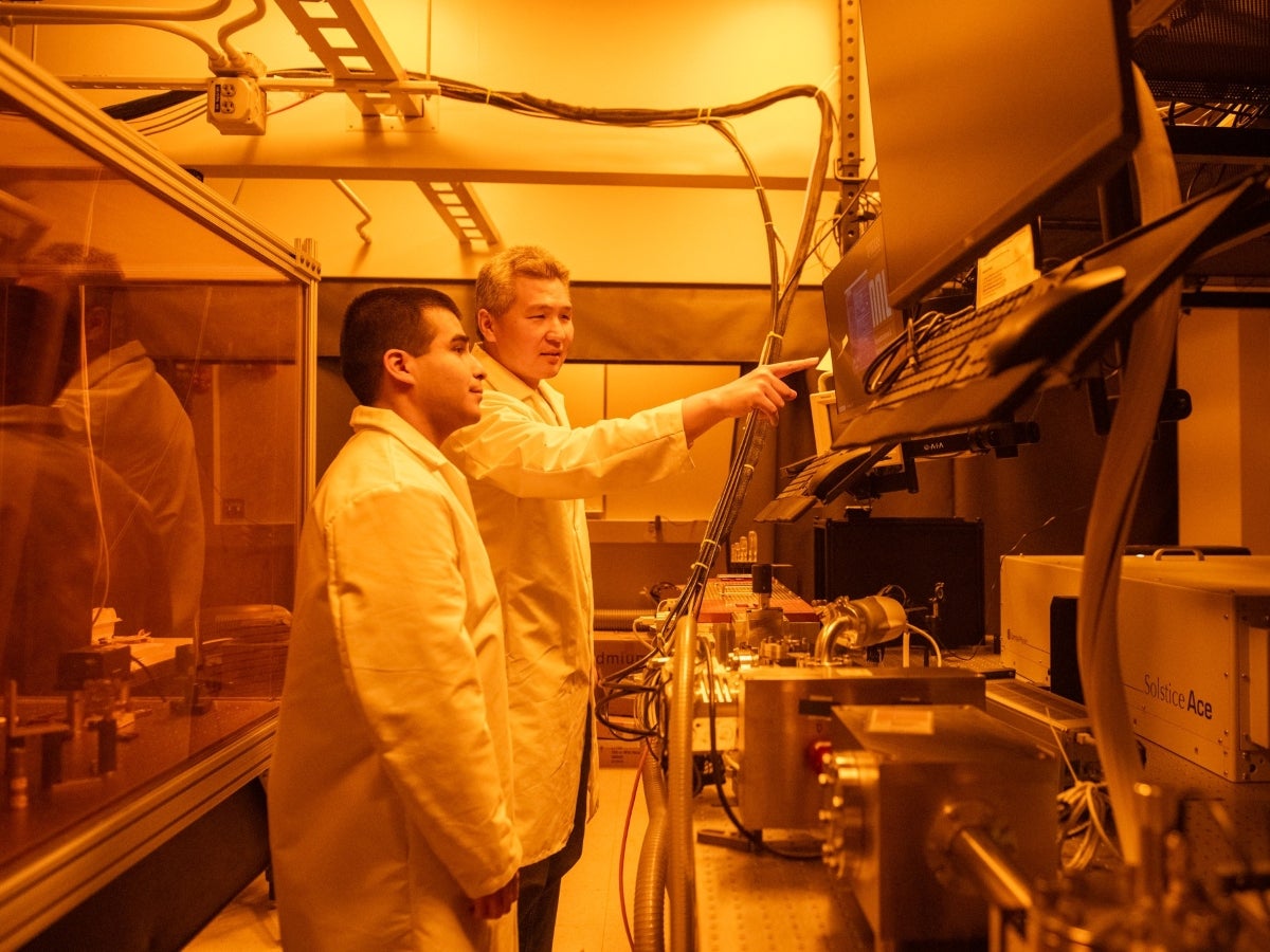
Customary EUV lithography machines value greater than $200 million and occupy a complete room, placing industrial semiconductor manufacturing out of attain for many analysis establishments. The Cockrell Faculty crew stripped the normal printer all the way down to its primary elements, producing a modular, inexpensive system that sits on a desk. It’s a significant shift for educational researchers who can’t entry industrial-scale tools.
The method, known as volumetric 3D patterning, solves a persistent bottleneck. Industrial EUV lithography can solely print 3D nanostructures in 2D steps, one layer at a time. The brand new strategy prints a number of layers concurrently. “The precise printing won’t take very lengthy,” mentioned Chih-Hao Chang, a professor within the Walker Division of Mechanical Engineering and one of many lead authors on the paper. “However the processing can take days.”
The analysis is funded by way of the Nationwide Science Basis’s Way forward for Semiconductors (FuSe2) program, which targets value discount in semiconductor analysis. The Cockrell crew has already examined an EUV materials developed by companions at UT Dallas and Johns Hopkins College, with extra assessments deliberate.
Proper now, the system can solely sample periodic buildings, making it most helpful for reminiscence chips and photonics. The longer-term aim is quicker printers able to producing extra complicated options for smaller transistor switches, giving particular person chips higher computing energy. “Past semiconductor manufacturing, the flexibility to sample 3D nanostructures can discover purposes in medication for nanodrugs, quantum computing or synthesizing novel supplies,” mentioned Saurav Mohanty, a current Ph.D. graduate and the research’s first writer.
Supply: cockrell.utexas.edu